
Hardware architecture
The required devices to support satellite channel emulation are the NI PXIe-8135 and the NI PXIe-5644R. The NI PXIe-8135 is a high-performance Intel Core i7-3610QE processor-based embedded controller which implements the thermal noise and delay effects. It also controls the NI PXIe-5644R which includes the needed radiofrequency functionality to down-convert the received QPSK signal, perform signal sampling in the baseband domain for further processing and regenerate the radiofrequency signal. The front panel of the NI PXIe-5644R can be observed in Figure 1. The radiofrequency input and output provide independent local oscillators, frequency coverage from 65 MHz to 6 GHz, and sampling frequency of up to 80 MHz.
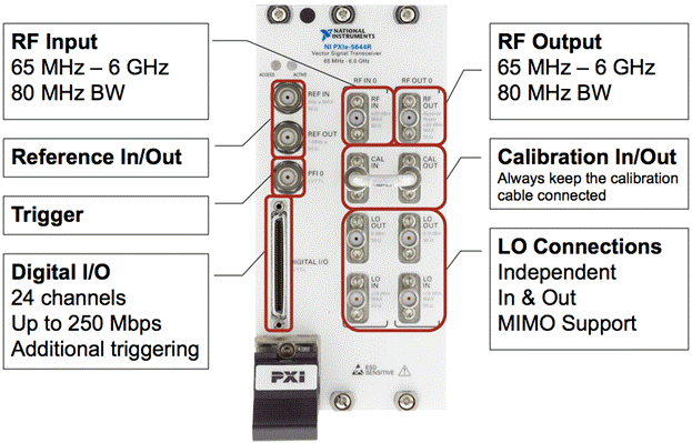
Figure 1. NI PXIe 5644R front panel
Due to the fact that the modems operate in L-band (1-2 GHz) transmitting data at 2 Mbauds, the use of NI PXIe-5644R results in an affordable solution for satellite channel emulation. Figure 2 depicts the tasks carried out by the NI devices to process the incoming QPSK signal.
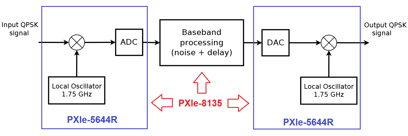
Figure 2. Signal processing scheme
Besides that, the NI PXIe-5644R also provides an integrated LabView programmable FPGA which enables high power processing. In this project, the signal processing is executed in the NI PXIe-8135 instead of the FPGA due to time constraints.
Software architecture
To order to control the vector signal analyzer (VSA) and the vector signal generator (VSG) of the NI PXIe-5644R and perform the signal processing a source code is developed in LabView which is installed in the NI PXIe-8135.
The LabView development is mainly based on the VST Streaming project and the previous QPSK implementation functions such as the noise generation, the delay effect and the visualization tools.
The front panel is illustrated in Figure 3, the following features are provided
- $Eb/No$ level [dB]
- Time delay [ms]
- Input/Output frequency carrier [GHz]
- Sampling frequency [MHz]
- Power spectral density
- Eye diagram
- Symbol constellation
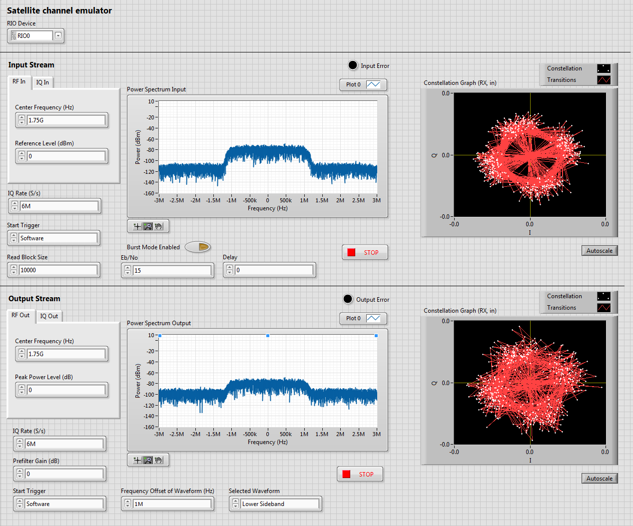
Figure 3. Emulator front panel
On the other hand, the whole block diagram implementation consist of five major parts which will be explained below
- PXIe-5644R initialization and configuration
- Acquisition of the QPSK signal
- Noise and delay generation
- Streaming of the channel-applied signal
- Visualization and monitoring
PXIe-5644R initialization and configuration
The initialization and configuration of the VST is shown in Figure 4. The VST local oscillator (LO) is configured to operate at the required frequency and the trigger function is set up to ensure synchronized samples across the RF inputs and outputs of the VST at a given sampling rate. This block also downloads the FPGA bitfiles on the VST for execution.
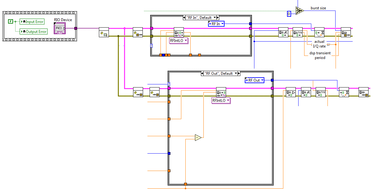
Figure 4. Device initialization and configuration
Acquisition of the QPSK signal
In Figure 5, it can be seen how the acquisition loop reads the samples stored in a Direct Memory Access (DMA) buffer. A DMA channel is composed of two FIFO buffers: one on the computer side and another one on the FPGA side. Therefore, in order to recover the QPSK samples, a function block writes data from the FPGA to the DMA buffer and another function block on the computer side reads the data from the target buffer.
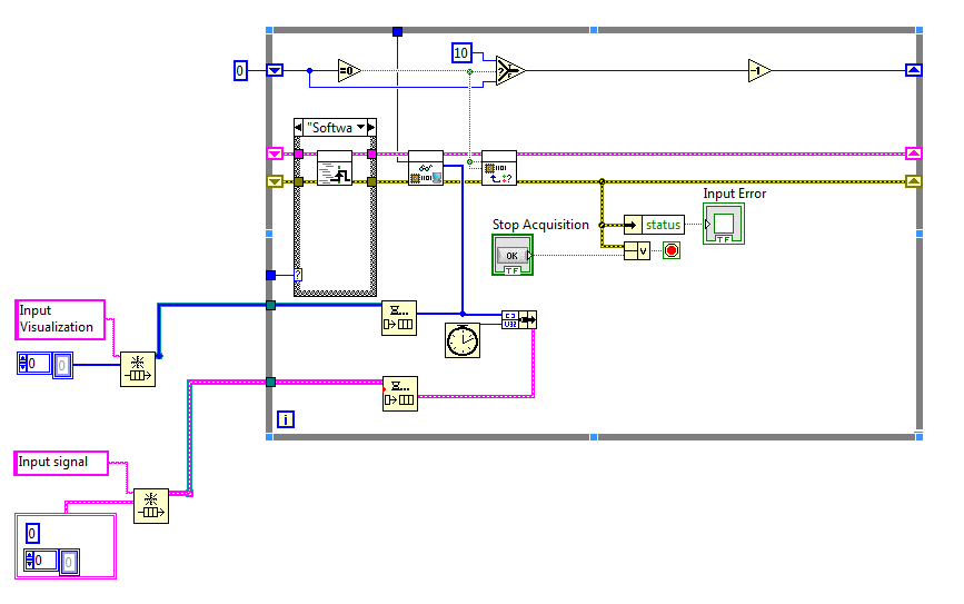
Figure 5. Data acquisition
Since the unsigned 16-bit integer format is used to represent the samples, a function converts these samples into complex symbols in order to reuse the functions developed in the previous implementation.
Once the data is formatted, the samples are added to a FIFO queue. As in the previous LabView development, the queue approach is implemented to connect the main function loops.
Noise and delay generation
After removing the complex symbols from the queue, the signal power is calculated in order to determine the required noise power for a given $Eb/No$ value that is selected by the user. So that, a noise signal is generated and added to the complex one as shown in Figure 6.
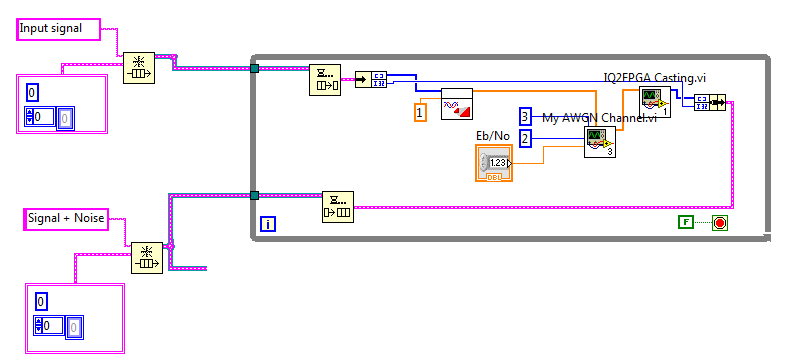
Figure 6. Noise generation
In order to create a time delay $t_d$ in the transmission, the noisy samples must wait in the loop for a period of $t_w$ before being delivered to the DMA buffer. As explained later, it must be noticed that the total delay generated by the emulator comprises the required delay as well as the processing time performed in the VST.
Therefore, the waiting time $t_w$ is calculated as follows
$t_w = t_d - (t_n - t_a)$
where t_a represents the time when the samples are acquired from the DMA buffer and t_n represents the time when the noisy samples are received in the output loop. The term $(t_n - t_a)$ corresponds to the processing time that must be removed from the required delay.
Considering the mentioned aspects, the data transmission to the DMA buffer is delayed by $t_w$ once when the first cluster of symbols is received in the output loop queue. The block diagram implementation can be observed in Figure 7.
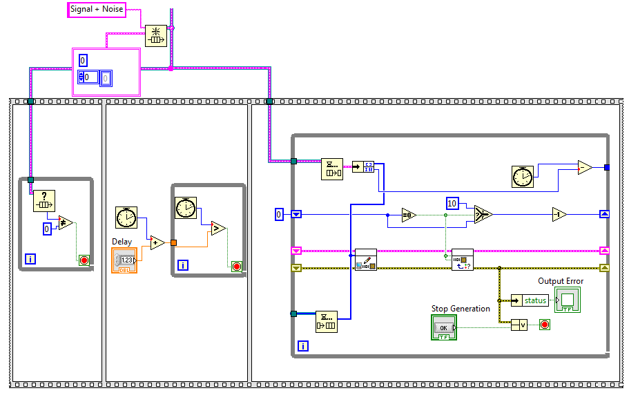
Figure 7. Delay generation
Streaming of the channel-applied signal
Finally, the channel-applied signal samples are dequeued and written to the DMA buffer in order to be converted from a digital format to an analog signal as shown in Figure 8. These samples are interpolated via a DAC, subsequently, the analog signal is up-converted to the required frequency carrier.
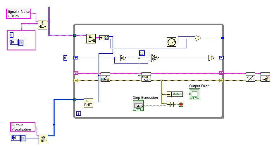
Figure 8. Data streaming
Visualization and monitoring
In order to analyze the transmitted signal, the symbol constellation, the eye diagram and the power spectral density of the QPSK signal are plotted. These loops are executed in parallel to exploit the multiprocessor computing power. As can be observed in Figure 9, there are two visualization and monitoring loops: one before and another after the channel.
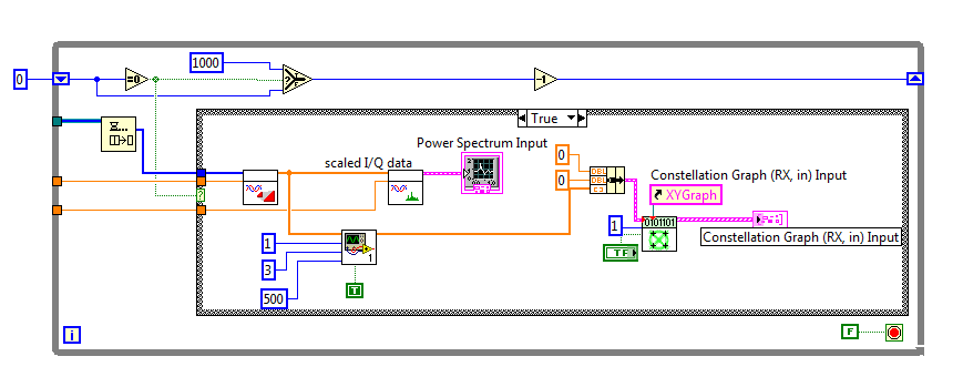
Figure 9. Monitoring loop