System Integration
The system we are proposing in order to achieve the objectives we defined, is composed by the following subsystems :- The development board (DB)
- The DSPIC33F microprocessor of Microchip / Analog-to Digital Converter (ADC)
- The thermocouple
- LEDS to monitor the state of the program
- The 2-FSK RF transimter
- We are developing on the development board rather than the motherboard in order to test and validate our system.
- As it is in a testing phase, we we also have the In-Circuit-Debugger ICD3 and our computer
The DSPIC33D is monted on the development board. We are using the Cubesat bus in order to connect the different equipment.
We are using the ADC already installed in the DSPIC33F to measure the difference of voltage in the thermocouple and to software-transform it in temperature.
The DB is fed by a power source, and the ICD3 is fed by the computer.
Sub-systems
LEDs
We are using standard 5 mm diameter red LEDs as monitors during the unfolding of the program.
We are connecting them on the BUS connector, with their input side on I/O port 47,43,39,35, 31 and 29 and their output on I/O ports 46,42,38,34,30. During the program, setting the inputs I/O ports to high would turn on the LED, and to turn them to Low would turn them off
ADC
We are using the already integrated ADC to recover the voltage on each wire of the thermocouple.
The ADC is a device used to transform a continuous voltage to a digital bit stream. During the process, it has to quantify the analog input. We are taking advantage of that functionality so as to retrieve that quantification and reconvert it to voltage .
The ADC's principle is simple. Each ADC, (there is two of them on a DSPIC33F) samples the analog input it has been specified, during an interval of time wich cannot be smaller than 75 ns. After the sampling has been done, it begins the conversion to a 16-bit word, stored in a buffer.
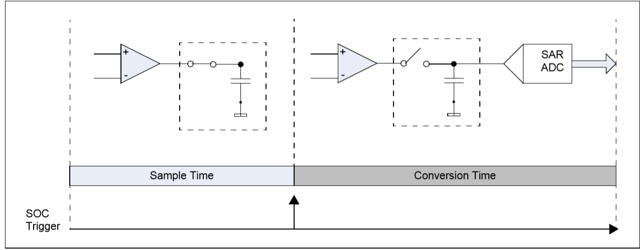
Figure : ADC sampling and conversion sequence
- ADxCON1 : ADCx Control Register 1 : this register contains the following interesting options
- ADON : ADC ON and OFF signal
- AD12B : 10-bit or 12-bit Operation Mode : the ADC constore data on 10 or 12 bits in the 16-bit buffer.
- FORM : Data ouput format : can be one of the following four:
- Signed fractional
- Fractional
- Signed integer
- Integer
- SSRC : Sample Clock Source Select : select if the clock of the ADC is internally or externally driven
- ASAM : ADC auto-Start : select wheter the sampling begins automatically after previuous conversion or when manually set
- DONE : the hardware store here a “1” when the conversion has been finished, and is reset automatically
- ADxCON2 : ADCx Control Register 2 : this register contains the following interesting options
- VCFG Converter Voltage reference Configuration :
- CHIPS : Channel select : the ADC can scan up to 4 channels (CH0, CH1, CH2, CH3), and we have to select which one(s) we want to use
- ADxCON3 : ADCx Control Register 3 : this register contains the following interesting options
- ADRC : ADC Conversion Clock source: internal or external
- SAMC auto sample Time : set the time taken to sample, as a multiple of a period "Tad", which is a period set by the system for unitary conversion and which can’t be lower than 75 ns
- ADC conversion clock : used to specify "Tad" by a calculation
- ADxCHS123 : ADCx Input Channel 1,2,3 Select : used to set the input and ouput of the channels 1,2 and 3, but won’t be used by us.
- ADxCHS0 : ADCx Input Channel 0 Select : we are to note here that each channel can buffer one input. It does that by defining "sample A" and "sample B", and then doing the conversion on either one of them alternatively. Here we will be using only the sample A. The register contains the following interesting fields :
- CH0NA : Channel 0 Negative Input select for sample A
- CH0SA : Channel 0 Positive Input select for sample A : for CH0S/NA, we select the analagog input to read
- ADxCSSH/L : ADCx Input scan select registers : used to select if the considered input are digitals or analog. If digital is selected, there won’t be any quantification possible with the
- ADCxPCFGH/L : ADCx Port configuration registers : used to select if the considered input are digitals or analog. If digital is selected, there won’t be any quantification possible with the ADC
RF Transmitter
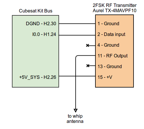
For the RF transmitter and the monopole antenna, we are simpling reusing what's was described in project Sputnik srikes back
The RF transmitter is a 2-FSK transmitter suited to ON-OFF modulations of digital signals. It has a serial input port and a RF out port for a dedicated antenna apart from power and ground port.
RF Transmitter pinout.
| Pin | Type | Function |
|---|---|---|
| 1 | G | Ground |
| 2 | I | Data input |
| 4 | G | Ground |
| 11 | O | RF output |
| 13 | G | Ground |
| 15 | P | +V |
Ground pins (1, 4 and 13) are internally interconnected.
Connection types: G = Ground, P = Power, I = Input, O = Output.
The interface between the motherboard and the transmitter is composed by the set of connections presented below.
Monopole antenna
From mission requirements and targeted objectives, the antenna must be omnidirectional. In addition, deployable wired antennas are well suited to Cubesats. For the scope of the project, a simple monopole whip antenna is appropriate.
Antenna design
A typical monopole quarter-wave antenna is built from a radiating wire whose length L is defined as follows:
L=c/(4fc)
Where fc is the carrier frequency and c the speed of light.
Since the carrier frequency of the 2-FSK modulator is 433.92 MHz, the required length of the wire is: L = 17.3 cm.
The figure belows shows the designed antenna to be mounted on the payload, connected to the RF transmitter.