System Integration
- Table of contents
- System Integration
- MCU (processor)
- Power management unit
- GPS receiver module
- 2-FSK RF transmitter
Processor and power management are considered as part of the Cubesat bus. On the other hand, the GPS receiver and RF transmitter are considered as part of the payload.
The implementation also includes a LED and a dedicated antenna for the RF transmitter. The GPS receiver is provided with an integrated active patch antenna. The system block diagram is presented below. Interfaces between main subsystems are identified as Int.1, Int.2, Int.3 and Int.4.
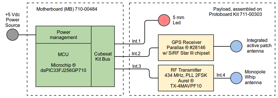
System diagram showing main subsystems and interfaces.
The Cubesat motherboard (MB) is fed by the power source, which is connected to the power management unit and provides power to all subsystems through the Cubesat Kit Bus.
In addition, the Cubesat Kit Bus (CKB) provides the interface for all communication paths between the processor (MCU) and subsystems.
The MCU provides all the processing and controlling capabilities of the system. It is responsible for communicating and handling all other subsystems. For the scope of the mission, the MCU is in charge of recollecting data from the GPS subsystem, then formatting it, and finally sending the beacon message by controlling the physical layer.
Subsystems and interfaces description
LED and Interface 1
The LED is a typical 5 mm diameter red LED, which requires between 3 and 10 mA in ON state.
The figure below presents the schematic of the circuit and the interface (Int.1) connections, which represents the connections with the CKB. The resistor R1 in series with the LED limits the polarization current to 10 mA approximately.
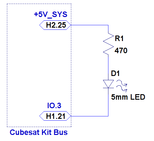
LED connection schematic.
GPS module and Interface 2
The GPS module includes an active patch antenna. The device computes ranging and constellation related information, in order to provide GPS data through the serial port. Information can be retrieved in two different modes: Raw and Smart modes.
The ports of the GPS receiver module are presented below (from the device datasheet).
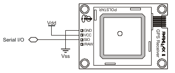
GPS Receiver pinout.
| Pin | Name | Type | Function |
|---|---|---|---|
| 1 | GND | G | System ground. Connect to power supply’s ground (GND) terminal. |
| 2 | VCC | P | System power, +5V DC input. |
| 3 | SIO | I/O | Serial communication (commands sent TO the Module and data received FROM the Module). Asynchronous, TTL-level interface, 4800 bps, 8 data bits, no parity, 1 stop bit, non-inverted. |
| 4 | /RAW | I | Mode select pin. Active LOW digital input. Internally pulled HIGH by default. When the /RAW pin is unconnected, the default “Smart Mode” is enabled, wherein commands for specific GPS data can be requested and the results will be returned. When /RAW in pulled LOW, the Module will enter “Raw Mode” and will transmit standard NMEA0183 strings, allowing advanced users to use the raw information directly. |
Connection types: G = Ground, P = Power, I = Input, O = Output.
The operating mode chosen is the Raw Mode since it provides already formatted strings in standard NMEA0183, which allows to save processing resources compared to the Smart Mode which would require a polling strategy from the MCU to get the data and then the string formatting. Therefore, the /RAW pin must be pulled down.
The electronic interface between the GPS module and the motherboard (MB) specifies the required connection in order to operate and/or communicate with the device.
Since in Raw Mode the GPS module transmits continuously data through an USART bus, the SIO pin must be connected to one of the USART Rx ports of the MCU. Then, the set of connections with the Cubesat Kit Bus are presented below.
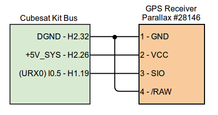
Motherboard-GPS interface.
RF Transmitter and Interface 3
The RF transmitter is a 2-FSK transmitter suited to ON-OFF modulations of digital signals. It has a serial input port and a RF out port for a dedicated antenna apart from power and ground port.
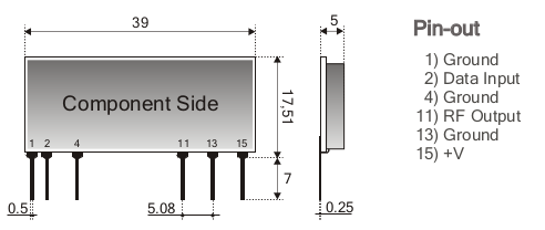
RF Transmitter pinout.
| Pin | Type | Function |
|---|---|---|
| 1 | G | Ground |
| 2 | I | Data input |
| 4 | G | Ground |
| 11 | O | RF output |
| 13 | G | Ground |
| 15 | P | +V |
Ground pins (1, 4 and 13) are internally interconnected.
Connection types: G = Ground, P = Power, I = Input, O = Output.
The interface between the motherboard and the transmitter is composed by the set of connections presented below.
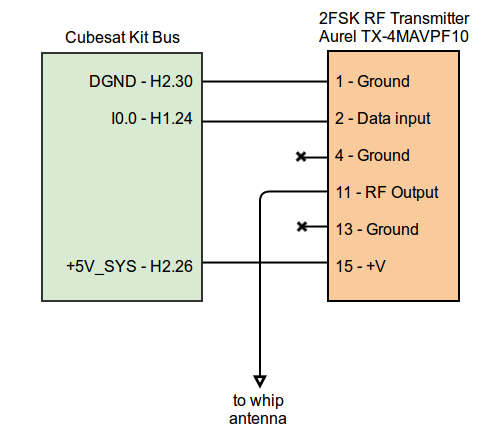
Motherboard-RF Transmitter interface.
Monopole antenna and Interface 4
From mission requirements and targeted objectives, the antenna must be omnidirectional. In addition, deployable wired antennas are well suited to Cubesats. For the scope of the project, a simple monopole whip antenna is appropriate.
Antenna design
A typical monopole quarter-wave antenna is built from a radiating wire whose length L is defined as follows:
$L = c / (4 f_c)$
Where $f_c$ is the carrier frequency and $c$ the speed of light.
Since the carrier frequency of the 2-FSK modulator is 433.92 MHz, the required length of the wire is: L = 17.3 cm.
The figure belows shows the designed antenna to be mounted on the payload, connected to the RF transmitter.

Monopole wired antenna.
Payload integration and assembly
The payload is mounted in the Protoboard Kit 711-00303, which is provided with the Cubesat Kit Bus connectors. The figure presented below shows the board footprints and the location of subsystem modules.
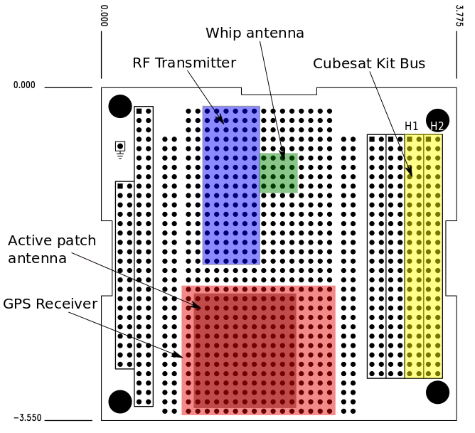
Payload layout.
Since no complex circuit connections are required, the integration is done only with wires and Female-Male pin connectors. This allows to reuse the board and devices in further projects.
The first picture presented below shows the payload integrated on the protoboard, mounted over the motherboar performing a test. The last picture shows the payload with the motherboard both assembled with the Cubesat chasis.
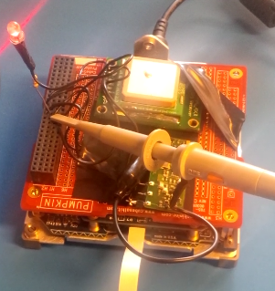
Payload integration over the motherboard performing a test.
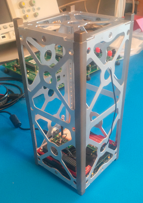
Payload and motherboard assembled with the Cubesat chasis.
