Integration » History » Version 7
« Previous -
Version 7/21
(diff) -
Next » -
Current version
PRIETO, Matías, 03/22/2015 01:06 AM
Integration
- Table of contents
- Integration
- MCU (processor)
- Power management unit
- GPS receiver module
- 2-FSK RF transmitter
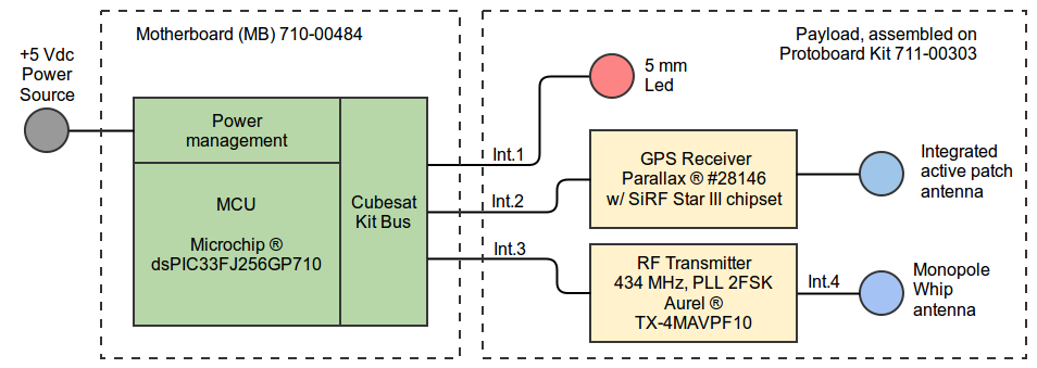
Processor and power management are considered as part of the Cubesat bus. On the other hand, GPS receiver and RF transmitter is considered as part of the payload.
The implementation also includes a LED and a dedicated antenna for the RF transmitter. GPS receiver is provided with an integrated active patch antenna. The system block diagram is presented below. Interfaces between main subsystems are identified as Int.1, Int.2, Int.3 and Int.4.

System diagram showing main subsystems and interfaces.
The Cubesat motherboard (MB) is fed by the power source, which is connected to the power management unit and provides power to all subsystems through the Cubesat Kit Bus.
In addition, the Cubesat Kit Bus (CKB) provides the interface for all communication paths between the processor (MCU) and subsystems.
The MCU provides all the processing and controlling capabilities of the system. It is responsible to communicate and handle all other subsystems. For the scope of the mission, the MCU is in charge of recollecting data from the GPS subsystem, then formatting it to finally send the beacon message by controlling the physical layer behavior.
Subsystems and interfaces description
LED and Interface 1
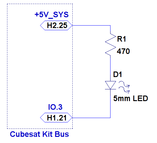
The LED is a typical 5 mm diameter red LED, which requires between 3 and 10 mA in ON state.
The figure below presents the schematic of the circuit and the interface (Int.1) connections, which represents the connections with the CKB. The resistor R1 in series with the LED limiting the polarization current to 10 mA approximately

LED connection schematic.
GPS module and Interface 2
The GPS module includes an active patch antenna. The device computes ranging and constellation related information, in order to provide GPS data through the serial port. Information can be retrieved in two different modes: Raw and Smart modes.
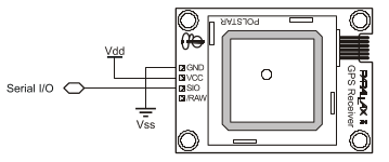
The electronic ports of the GPS receiver module are presented below (from the device datasheet).

GPS Receiver pinout.
| Pin | Name | Type | Function |
|---|---|---|---|
| 1 | GND | G | System ground. Connect to power supply’s ground (GND) terminal. |
| 2 | VCC | P | System power, +5V DC input. |
| 3 | SIO | I/O | Serial communication (commands sent TO the Module and data received FROM the Module). Asynchronous, TTL-level interface, 4800 bps, 8 data bits, no parity, 1 stop bit, non-inverted. |
| 4 | /RAW | I | Mode select pin. Active LOW digital input. Internally pulled HIGH by default. When the /RAW pin is unconnected, the default “Smart Mode” is enabled, wherein commands for specific GPS data can be requested and the results will be returned. When /RAW in pulled LOW, the Module will enter “Raw Mode” and will transmit standard NMEA0183 strings, allowing advanced users to use the raw information directly. |
Connection types: G = Ground, P = Power, I = Input, O = Output.
