PRELIMINARY TESTS
In order to get in touch with the equipment, a series of simple tests were carried out, à la “hello world”. These tests were carried out on the Development Board, taking advantage of the documentation and sample software provided by the manufacturer. After reading the documentation concerning the DB, the MCU and the operating system, we proceeded with the testing.
The first test, was carried out to check the programmer and the provided OS (Salvo RTOS). The program, consisted of a output pin switching every 5 seconds, from which a LED was connected. The test was successful.
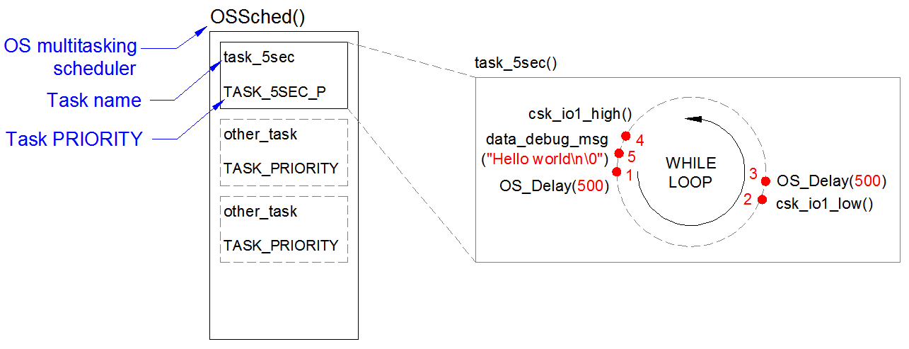
Diagram showing the operation of the test program.
The next test, was aimed to check the communication between a PC and the MCU. Using the same task repeated every 5 seconds, a message with a baudrate of 9600 was sent through the UART connected to the USB (through the FTDI chip). The messages were successfully received on a PC.
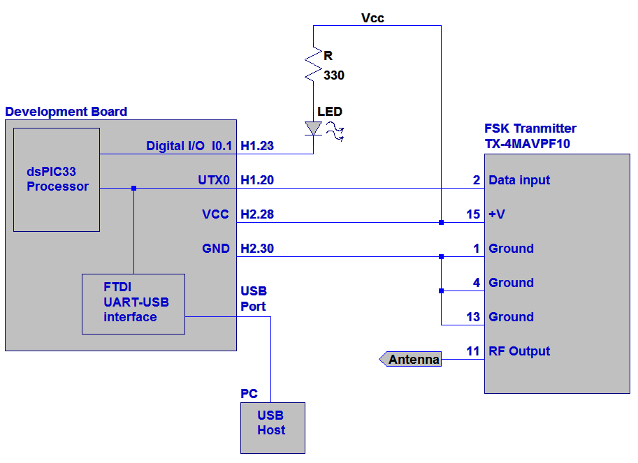
Connections diagram.
Finally, a test was made to check the operation of the RF transmitter. To accomplish such task, the transmitter was connected to the MCU through the same UART used in the previous test. Lacking an appropriate receiver capable of demodulating the message, the checking was made measuring the signal at the antenna output pin with an oscilloscope, and measuring the emitted power with a spectrum analyzer. The results showed that power was being transmitted in the frequencies corresponding to a logic 0 and logic 1, so the test was considered successful.
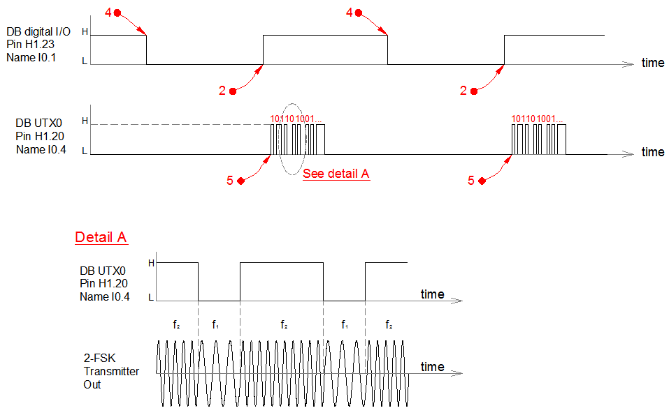
Diagram of signals measured at the output of the UART and the output of the transmitter.
It has been performed a set of laboratory measures with different instruments in order to validate the correct operation of the communication chain described above.
Set of testing procedures:- Firstly, before powering on the devboard, it was performed the measurement of the correct connectivity between IN-OUT ports, with the multimeter.
- Then, the system was switched on, and it was performed the measurement of the correct polarisation levels at the Vcc and GND ports of the RF transmitter, with the multimeter.
- Additionally, it was performed the measurement of the signals in the time domain with the oscilloscope. These measures were taken in the UART link between the processor and the RF transmitter (serial input at the RF module), and the RF output port of the RF transmitter. The captures are presented below, showing the expected correct operation.
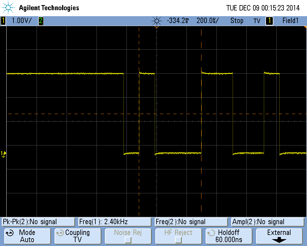
Oscilloscope Capture: signal in the UART link between the processor and the RF transmitter
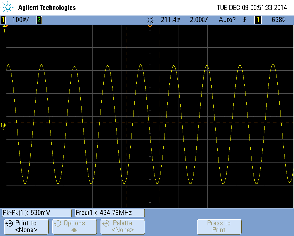
Oscilloscope Capture: signal in the RF output port at RF transmitter
- Finally, it was performed the measurement of the RF output signal spectral characteristics with a spectrum analyser. The results let us capture the carrier when no signal was transmitted and the typical 2-FSK spectrum shape when a signal was transmitted. The captures are presented below.
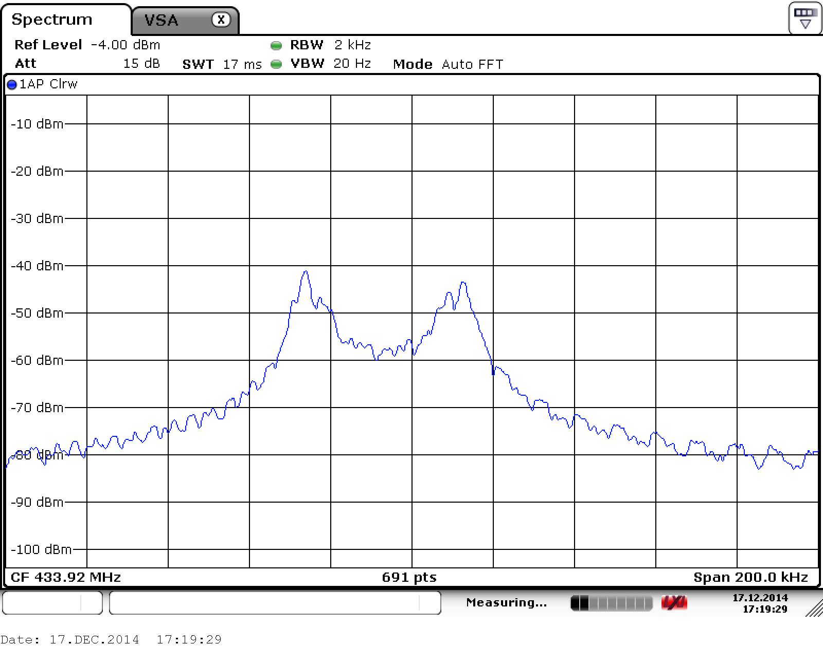
Spectrum Analyser Capture: Typical 2-FSK spectrum
At the end of this series of tests, the familiarization with the equipment was deemed completed, so the mission analysis stage was started. Further testing is expected to be done when the final prototype is developed.
